
The Setup: Advanced Packaging Stocks
"Our packaging capacity is so tight that now it limits my customers' growth."
That was TSMC's C.C. Wei in July, answering an analyst who'd asked about a rival's packaging technology. The head of the world's most important chipmaker didn't trash the competition. He welcomed it, because he can't build enough of the stuff himself.
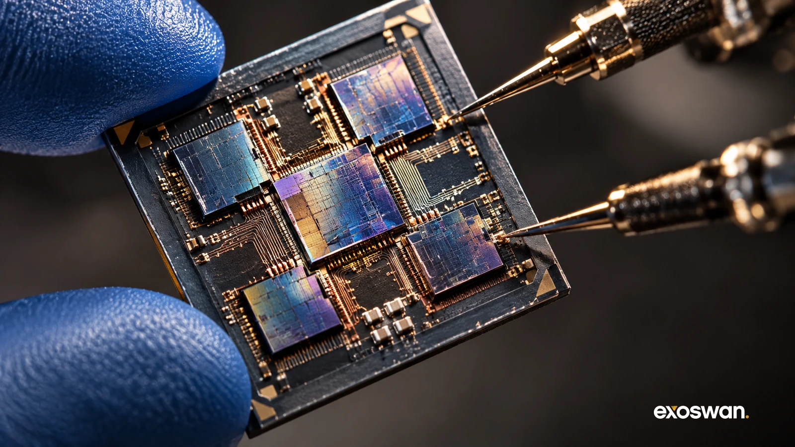
That's where the AI chip shortage has moved. Printing the chips isn't the hard part anymore. Putting them together is, and that's the job advanced packaging does. An AI accelerator isn't one chip. It's a few logic dies and a ring of high-bandwidth memory stacks, packed side by side or on top of each other so tightly they behave like one giant processor. The package used to be the plastic shell around a chip. Now it decides how fast the whole thing runs, and only a handful of factories on Earth can build one. (You'll also hear it called chiplet packaging, or CoWoS if you're TSMC.)
Relief is coming, just not soon. The big new plants and U.S. sites mostly reach volume in 2028, which makes 2027 another year of rationing, and for advanced packaging stocks, rationing pays whoever holds the capacity.
We've grouped these advanced packaging stocks by where each company sits in that shortage: the bottleneck itself, the overflow that catches what TSMC can't, the toolmakers adding capacity, the inspectors protecting yield, and the material that runs short next.
Companies at a glance
10 companies| Company | Ticker | Segment | Thesis |
|---|---|---|---|
| TSMC | NYSE: TSM | Bottleneck | The line every AI chip waits in |
| ASE Technology | NYSE: ASX | Overflow | Gets to panels first |
| Amkor Technology | NASDAQ: AMKR | Overflow | Customers are prepaying for its capacity |
| Intel | NASDAQ: INTC | Overflow | One big packaging customer away from a turnaround |
| Applied Materials | NASDAQ: AMAT | Toolmakers | Paid whichever bonding method wins |
| ASMPT | HKEX: 0522 | Toolmakers | The overflow, turned into bonder orders |
| BE Semiconductor | Euronext Amsterdam: BESI | Toolmakers | The right technology on a later clock |
| Onto Innovation | NYSE: ONTO | Yield Keepers | Next year is already in the backlog |
| Camtek | NASDAQ: CAMT | Yield Keepers | Orders running ahead of revenue |
| Ibiden | TYO: 4062 | Next Shortage | Where the squeeze goes after packaging |
Bottleneck
One company sets the pace for nearly every AI chip on the market.
TSMC NYSE: TSM
TSMC is the only company that prints leading-edge logic and packages it under the same roof. That bundle is why its CoWoS process became the default way to build an AI accelerator. It's also why the shortage sits here: Nvidia, AMD, and every custom-chip program are queued for the same back-end lines.
TSMC is spending its way out, with this year's capex budget raised to $60–64 billion and another $100 billion pledged for Arizona that includes packaging plants. It's also doing something monopolies rarely do, which is ask for help. It signed a 10-year deal to buy packaging from Amkor, and its CEO is publicly cheering on Intel's alternative.
Overflow
When TSMC can't take the work, it flows to the companies that handle the less glamorous end of chipmaking, plus one that badly needs the business.
ASE Technology NYSE: ASX
ASE is the world's largest outsourced packaging house, and the shortage has turned it from TSMC's junior partner into its pressure valve. Its leading-edge packaging revenue is running ahead of a $3.5 billion target for 2026.
The more interesting story is shape. ASE is building a 310mm-square panel line due to start production in the first half of 2027. AI packages have grown so large that round wafers waste space at the edges, and square panels fit more of them. TSMC's own panel effort isn't expected at volume before 2028, so if panels work, ASE gets there first.
Amkor Technology NASDAQ: AMKR
Amkor is becoming America's answer to the shortage. In June, TSMC signed a 10-year agreement to buy packaging from Amkor's campus near TSMC's own fabs in Arizona.
A month later, a customer agreed to hand Amkor about $1.5 billion in advance payments in 2027. The filing doesn't name the customer; press reports say it's Nvidia. Either way, nobody prepays for something they expect to be plentiful.
Intel NASDAQ: INTC
Intel is the turnaround on this list, and packaging might be the piece of the turnaround that works first. Its EMIB-T technology links chips with small silicon bridges instead of the full silicon interposer CoWoS uses, and it scales to very large packages. It's the alternative TSMC's CEO said the market could use.
Intel says its EMIB-T backlog is growing and yields are on target, but it hasn't named a major outside customer.
That announcement is the whole bet. One hyperscaler packaging TSMC-made chips at Intel would prove Intel can sell manufacturing to companies that buy their chips from its biggest rival.
Toolmakers
Every new packaging line needs machines, so these companies see the shortage in their order books before anyone sees it in chip supply. That makes them the earliest read on the shortage among advanced packaging stocks.
Applied Materials NASDAQ: AMAT
Applied Materials is the broad way to own packaging equipment without picking a technique. It sells the plating, polishing, deposition and inspection steps every advanced package goes through, however the dies end up bonded.
Management now expects packaging revenue to grow more than 70% this year, up from a forecast of more than 50% a quarter earlier. It has also been buying in: ASMPT's panel-plating business closed in June, and Applied owns about 9% of Besi.
ASMPT HKEX: 0522
ASMPT makes thermo-compression bonders, the machines that press chips onto substrates and stack today's memory. In July it booked bulk orders for more than 50 chip-to-substrate bonders from outsourced packaging houses. That's TSMC's overflow showing up as equipment demand, and it's why second-quarter bookings nearly doubled from a year earlier.
BE Semiconductor Industries Euronext Amsterdam: BESI
Besi is the bet on what replaces today's bonders. Hybrid bonding fuses copper straight to copper with no solder bumps, so chips sit closer and talk faster on less power. Besi is the company most tied to it, and its hybrid-bonding customer count went from 15 to 21 in the first half of 2026, including a new hyperscaler.
Timing is the thesis here. The industry loosened the height limit on memory stacks, and in August SK hynix said hybrid bonding for memory waits until HBM5, which pushes the big memory ramp toward 2028. Until then, Besi has to grow on logic chips and optics, and so far it has.
Yield Keepers
A finished AI package carries tens of thousands of dollars of silicon, and a defect found at the end scraps all of it. Every new layer of complexity is a sale for inspection.
Onto Innovation NYSE: ONTO
Onto sells the inspection and measurement tools that catch packaging defects before they get expensive. A leading memory maker picked its Dragonfly platform for HBM4, and the same tool is qualified for the 2.5D packages AI accelerators use.
The tell is the backlog. It crossed $1 billion for the first time this summer, at a company doing about $350 million a quarter in revenue. A good chunk of 2027 is already booked.
Camtek NASDAQ: CAMT
Camtek is the smaller, more concentrated inspection name, with growth tied to advanced packaging and memory stacks. Its revenue grew just 8% last quarter. Its orders tell a different story: more than $600 million booked this year by August, including over $105 million scheduled for delivery in 2027.
Camtek runs a few quarters behind the shortage, so much of that order book turns into revenue next year.
Next Shortage
Fix the packaging line and the bottleneck moves down a layer, to the board every package sits on.
Ibiden TYO: 4062
Ibiden makes the high-end substrates AI accelerators are mounted on, the layered boards that route thousands of connections from the chip to the rest of the server. Intel said this summer it's facing one of the worst supply crunches in its history, across wafers, memory and substrates.
Ibiden has committed hundreds of billions of yen to new capacity, but it comes online in stages starting in 2027. The specialty glass fiber inside these boards is tight too. If packaging capacity catches up first, this is where the shortage goes next.
The Future of Advanced Packaging
For the whole AI boom so far, the package came bundled. You paid TSMC to print the chip, TSMC packaged it, and that bundle was a big reason nobody could leave.
The shortage is breaking the bundle. TSMC now buys packaging from Amkor. Intel is pitching its bridges to companies whose wafers come from TSMC. Outsourced packaging houses are building CoWoS-class plants of their own, and ASE is moving to panels ahead of TSMC.
When the new capacity lands in 2028, the shortage will ease. The habits customers picked up during it won't. A chip designer who has learned to pair one company's wafers with another's package has leverage, and won't give it up.
That turns advanced packaging from a step inside the foundry into a market of its own, with its own pricing and its own competition. The shortage is the 2027 trade for advanced packaging stocks. The unbundling is what outlasts it.